愛彼電路 - 值得信賴的PCB電路板製造企業!聯絡我們


隨著科學技術的進步,電子產品已成為人們生活中不可或缺的日常用品,而PCB是電子產品的重要組成部分。 近年來,人們對電子產品的功能要求越來越高,這對PCB提出了更高的要求。 通常,為了便於在PCB上安裝特殊功能器件或下沉器件,通常需要在PCB上設定PCB階梯槽。 PCB階梯槽也是產品大功率散熱的重要組成部分,在PCB加工行業中應用廣泛。
現時,製作PCB梯形槽的方法主要有兩種
一種是控制深度銑削的製造方法。 這種生產方法不僅難以控制深度,難以將深度銑削控制到指定的線層,導致無法滿足設計要求,而且無法在凹槽底部製作圖形。
另一種是填充或嵌入墊圈。 這種製造方法很容易出現分層空腔現象。 這是由於在層壓過程中,鋼板會擠出PCB臺階凹槽中的部分空氣,產生一定的擠出壓力,導致墊圈移位,在芯板和槽邊緣的半固化片之間鑽孔,取出墊圈後形成空腔。 這種空腔會降低PCB的可靠性,孔位置的金屬電路會暴露出來,在應力作用下很容易分層。

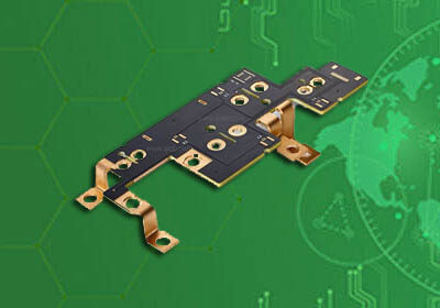
階梯槽PCB
階梯槽PCB具體規格可根據客戶要求,可製作階梯槽或階梯孔。
iPCB公司是一家專業生產高精度單面、雙面、多層PCB的高新技術企業。 生產層數為1-70層,小孔徑為0.075mm,線間距為1.5mil(0.03mm)。公司產品廣泛應用於航空航太PCB、通信PCB、光電PCB、工控PCB、儀器儀錶PCB、汽車PCB、各類家電PCB, iPCB秉承“客戶至上、誠信、進取、共贏”的經營理念和“客戶至上,品質第一,全員參與,持續改進,追求卓越”的品質方針。 始終堅持“速度快、品質穩定、價格優惠、售後服務完善”,回饋新老客戶。 iPCB贏得了廣大客戶的支持和信任!
品名:階梯槽PCB
基板:FR-4 TG170
層別:4L
成品板厚:2.0mm
鍍銅厚度:1oz(35 μ m)
表面處理:化學金
最小線寬/線距:6/6 mil(150 / 150 μ m)
產品應用:多層PCB板,電源板
對於PCB技術問題,iPCB愛彼電路提供PCB技術的支持。 您也可以在這裡索取PCB報價或PCB諮詢。請聯繫郵箱: sales@ipcb.com
我們會非常迅速地做出回應。
